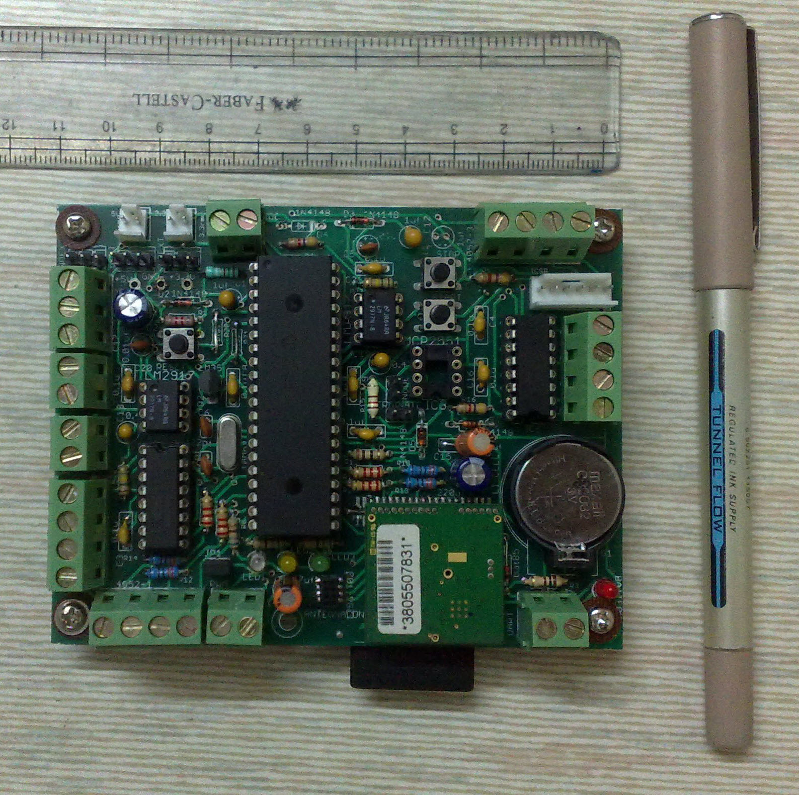
PCB design pointers/checklist
Pointers/Checklist to keep in mind while designing a new PCB.
- Include “Power ON” LED and LEDs for debug
- Include critical test points and extra VCC/GND railing/points
- Holes for Wire to hold xtal
- One way connectors only (RMC connectors)
- Easy access reset and other switch (check size of nearby components).
- Check if through hole components (especially 90 degree connectors) interfere with SMD/other components.
- Holes on corners for spacers (3mm-5mm dia)
- Space below and above ICs for removing IC from socket (if using an IC socket). Space for soldering iron, near bigger components like inductors and capacitors of power circuit
- 0.1uF ceramic caps between VCC and GND
- Everything on bottom layer should be mirror image (EAGLE top view)
- Through hole connectors offer more strength
- The rule of thumb for trace width is .010″[.0254] per 1 Amp external (normally 1.5 oz or .0021″[.0533]) and .040″[.1016] per 1 Amp internally (for 1/2 oz of copper)
- Check component availability before incorporating in design
- Use filled vias for heat dissipation in power circuits
- Are all IC inputs terminated as required?
- Do IC/components have necessary filter caps?
- Are main circuit and branch circuits clearly identified?
- Define board dimensions
- Define top and bottom board clearance for stacked/hierarchical PCB assembly
- Draw board border using .040″ line
- Define/determine a fixed component direction
- Add text to plane layer and to net names (GND, +5V, etc.).
- Board part number in copper on bottom side. Board revision (in copper or manually marking).
- For high current circuits, note current of branch circuits.
- Defining branch circuits and their current requirements is important if the main branch is of very high current. If the main branch requires a .050″[1.27] trace and the branches only require a .008″[.2032] width, it makes no sense to route all branches with a .050″[1.27] trace.
